- 您现在的位置:买卖IC网 > Sheet目录317 > C8051T610DB24 (Silicon Laboratories Inc)DAUGHTER BOARD T610 24QFN SOCKET
�� �
�
�C8051T610/1/2/3/4/5/6/7�
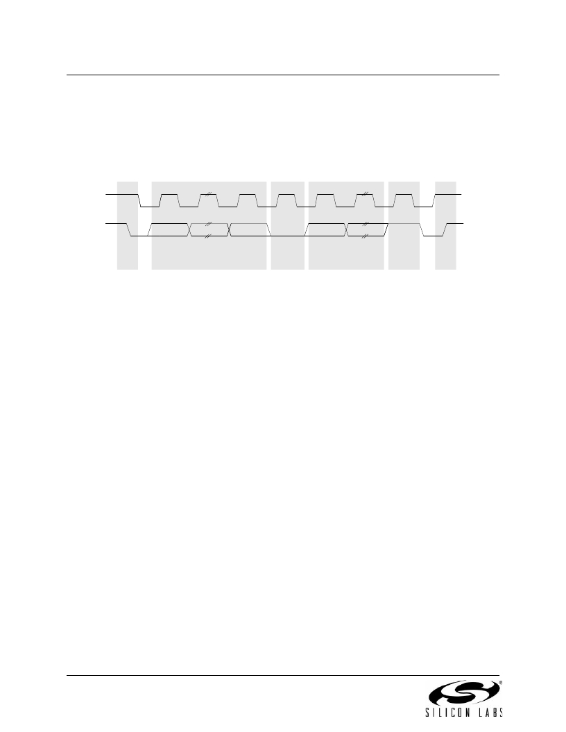
�All� transactions� are� initiated� by� a� master,� with� one� or� more� addressed� slave� devices� as� the� target.� The�
�master� generates� the� START� condition� and� then� transmits� the� slave� address� and� direction� bit.� If� the� trans-�
�action� is� a� WRITE� operation� from� the� master� to� the� slave,� the� master� transmits� the� data� a� byte� at� a� time�
�waiting� for� an� ACK� from� the� slave� at� the� end� of� each� byte.� For� READ� operations,� the� slave� transmits� the�
�data� waiting� for� an� ACK� from� the� master� at� the� end� of� each� byte.� At� the� end� of� the� data� transfer,� the� master�
�generates� a� STOP� condition� to� terminate� the� transaction� and� free� the� bus.� Figure� 22.3� illustrates� a� typical�
�SMBus� transaction.�
�SCL�
�SDA�
�SLA6�
�SLA5-0�
�R/W�
�D7�
�D6-0�
�START�
�Slave� Address� +� R/W�
�ACK�
�Data� Byte�
�NACK�
�STOP�
�Figure� 22.3.� SMBus� Transaction�
�22.3.1.� Transmitter� Vs.� Receiver�
�On� the� SMBus� communications� interface,� a� device� is� the� “transmitter”� when� it� is� sending� an� address� or�
�data� byte� to� another� device� on� the� bus.� A� device� is� a� “receiver”� when� an� address� or� data� byte� is� being� sent�
�to� it� from� another� device� on� the� bus.� The� transmitter� controls� the� SDA� line� during� the� address� or� data� byte.�
�After� each� byte� of� address� or� data� information� is� sent� by� the� transmitter,� the� receiver� sends� an� ACK� or�
�NACK� bit� during� the� ACK� phase� of� the� transfer,� during� which� time� the� receiver� controls� the� SDA� line.�
�22.3.2.� Arbitration�
�A� master� may� start� a� transfer� only� if� the� bus� is� free.� The� bus� is� free� after� a� STOP� condition� or� after� the� SCL�
�and� SDA� lines� remain� high� for� a� specified� time� (see� Section� “22.3.5.� SCL� High� (SMBus� Free)� Timeout”� on�
�page� 135).� In� the� event� that� two� or� more� devices� attempt� to� begin� a� transfer� at� the� same� time,� an� arbitra-�
�tion� scheme� is� employed� to� force� one� master� to� give� up� the� bus.� The� master� devices� continue� transmitting�
�until� one� attempts� a� HIGH� while� the� other� transmits� a� LOW.� Since� the� bus� is� open-drain,� the� bus� will� be�
�pulled� LOW.� The� master� attempting� the� HIGH� will� detect� a� LOW� SDA� and� lose� the� arbitration.� The� winning�
�master� continues� its� transmission� without� interruption;� the� losing� master� becomes� a� slave� and� receives� the�
�rest� of� the� transfer� if� addressed.� This� arbitration� scheme� is� non-destructive:� one� device� always� wins,� and�
�no� data� is� lost.�
�22.3.3.� Clock� Low� Extension�
�SMBus� provides� a� clock� synchronization� mechanism,� similar� to� I2C,� which� allows� devices� with� different�
�speed� capabilities� to� coexist� on� the� bus.� A� clock-low� extension� is� used� during� a� transfer� in� order� to� allow�
�slower� slave� devices� to� communicate� with� faster� masters.� The� slave� may� temporarily� hold� the� SCL� line�
�LOW� to� extend� the� clock� low� period,� effectively� decreasing� the� serial� clock� frequency.�
�22.3.4.� SCL� Low� Timeout�
�If� the� SCL� line� is� held� low� by� a� slave� device� on� the� bus,� no� further� communication� is� possible.� Furthermore,�
�the� master� cannot� force� the� SCL� line� high� to� correct� the� error� condition.� To� solve� this� problem,� the� SMBus�
�protocol� specifies� that� devices� participating� in� a� transfer� must� detect� any� clock� cycle� held� low� longer� than�
�25� ms� as� a� “timeout”� condition.� Devices� that� have� detected� the� timeout� condition� must� reset� the� communi-�
�cation� no� later� than� 10� ms� after� detecting� the� timeout� condition.�
�134�
�Rev� 1.1�
�发布紧急采购,3分钟左右您将得到回复。
相关PDF资料
C8051T630DB20
BOARD SOCKET DAUGHTER 20-QFN
CAN-100
BOARD EVAL RS232 100QFP
CANADAPT28
KIT ADAPTER CANDEMOBOARD 28PLCC
CAT24AA01WI-GT3
IC EEPROM SERIAL 1KB I2C 8SOIC
CAT24AA02WI-G
IC EEPROM SERIAL 2KB I2C 8SOIC
CAT24C01ZI-G
IC EEPROM SERIAL 1KB I2C 8MSOP
CAT24C03WI-G
IC EEPROM SERIAL 2KB I2C 8SOIC
CAT24C04ZI-G
IC EEPROM SERIAL 4KB I2C 8MSOP
相关代理商/技术参数
C8051T610DB28
功能描述:子卡和OEM板 C8051T610 Family Socket Daughtr Board RoHS:否 制造商:BeagleBoard by CircuitCo 产品:BeagleBone LCD4 Boards 用于:BeagleBone - BB-Bone - Open Source Development Kit
C8051T610DB32
功能描述:子卡和OEM板 C8051T610 Family Socket Daughtr Board RoHS:否 制造商:BeagleBoard by CircuitCo 产品:BeagleBone LCD4 Boards 用于:BeagleBone - BB-Bone - Open Source Development Kit
C8051T610DK
功能描述:开发板和工具包 - 8051 C8051T610 Series Development Kit RoHS:否 制造商:Silicon Labs 产品:Development Kits 工具用于评估:C8051F960, Si7005 核心: 接口类型:USB 工作电源电压:
C8051T610-GQ
功能描述:8位微控制器 -MCU 16KB 10ADC 32Pin MCU RoHS:否 制造商:Silicon Labs 核心:8051 处理器系列:C8051F39x 数据总线宽度:8 bit 最大时钟频率:50 MHz 程序存储器大小:16 KB 数据 RAM 大小:1 KB 片上 ADC:Yes 工作电源电压:1.8 V to 3.6 V 工作温度范围:- 40 C to + 105 C 封装 / 箱体:QFN-20 安装风格:SMD/SMT
C8051T610-GQR
功能描述:8位微控制器 -MCU 16KB 10ADC 32Pin MCU RoHS:否 制造商:Silicon Labs 核心:8051 处理器系列:C8051F39x 数据总线宽度:8 bit 最大时钟频率:50 MHz 程序存储器大小:16 KB 数据 RAM 大小:1 KB 片上 ADC:Yes 工作电源电压:1.8 V to 3.6 V 工作温度范围:- 40 C to + 105 C 封装 / 箱体:QFN-20 安装风格:SMD/SMT
C8051T611-GM
功能描述:8位微控制器 -MCU 16KB 10ADC 28Pin MCU RoHS:否 制造商:Silicon Labs 核心:8051 处理器系列:C8051F39x 数据总线宽度:8 bit 最大时钟频率:50 MHz 程序存储器大小:16 KB 数据 RAM 大小:1 KB 片上 ADC:Yes 工作电源电压:1.8 V to 3.6 V 工作温度范围:- 40 C to + 105 C 封装 / 箱体:QFN-20 安装风格:SMD/SMT
C8051T611-GMR
功能描述:8位微控制器 -MCU 16KB 10ADC 28Pin MCU RoHS:否 制造商:Silicon Labs 核心:8051 处理器系列:C8051F39x 数据总线宽度:8 bit 最大时钟频率:50 MHz 程序存储器大小:16 KB 数据 RAM 大小:1 KB 片上 ADC:Yes 工作电源电压:1.8 V to 3.6 V 工作温度范围:- 40 C to + 105 C 封装 / 箱体:QFN-20 安装风格:SMD/SMT
C8051T612-GQ
功能描述:8位微控制器 -MCU 8KB 10ADC 32Pin MCU RoHS:否 制造商:Silicon Labs 核心:8051 处理器系列:C8051F39x 数据总线宽度:8 bit 最大时钟频率:50 MHz 程序存储器大小:16 KB 数据 RAM 大小:1 KB 片上 ADC:Yes 工作电源电压:1.8 V to 3.6 V 工作温度范围:- 40 C to + 105 C 封装 / 箱体:QFN-20 安装风格:SMD/SMT